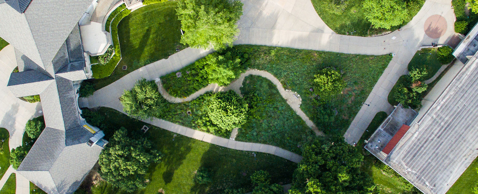
Research
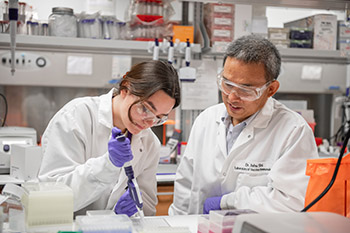
At Kansas State University, we believe research is more than labs and statistics — it's knowing the right questions to ask. Our expert faculty are constantly looking ahead for the next mystery to unravel or crisis to avert. Our mission to conduct research for the benefit of humanity propels us forward.
 Featured office
Office of Research Development
The Office of Research Development promotes and facilitates the research, education, and outreach missions of the university by supporting and administering activities involving extramurally sponsored programs.
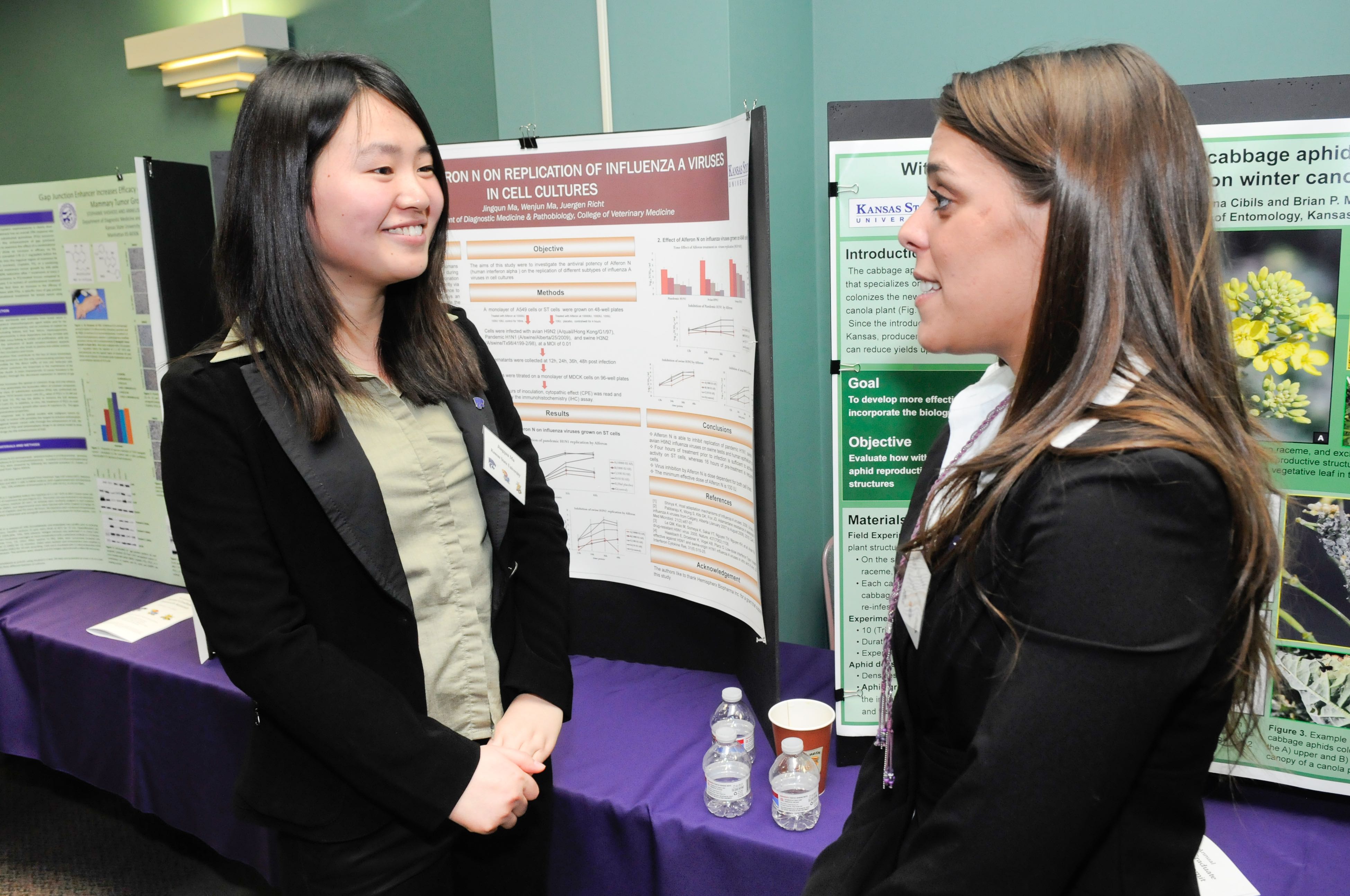
Undergraduate and graduate research opportunities
Academic discovery and creative inquiry are crucial to student success and preparation to enter the workforce — and not only at the graduate level. K-State offers many opportunities for undergraduate and graduate students to engage in research.
Collaborate with K-State
Become a strategic partner and leverage K-State's expertise, research and innovation.
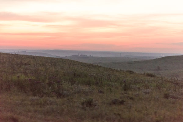
Featured Center
K-State is home to more than 90 research centers and institutes, including the Konza Prairie Biological Center. The Konza is located on a 3,487 hectare native tallgrass prairie preserve jointly owned by The Nature Conservancy and Kansas State University. The KPBS is located in the Flint Hills of northeastern Kansas (39°05’ N, 96°35’ W), a grassland region of steep-slopes overlain by shallow limestone soils unsuitable for cultivation.